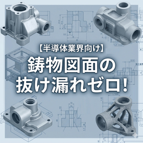
Points for Reviewing Methods to Reduce Costs in Design for the Semiconductor Industry
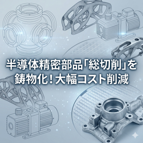
Shall we reconsider 'total cutting'? By using casting for near-net shape, we can reduce material loss and lower total costs.
In the precision parts of semiconductor manufacturing equipment, are "total cutting" and "welding assembly" putting pressure on costs? The selection of manufacturing methods at the design stage greatly influences production costs. ■ Main Factors Behind Rising Costs - Material Waste: Total cutting from sheet or block materials can result in more than half of the material being discarded as scrap. - Complexity of Processes: The processing and welding of multiple parts lead to increased processing costs and longer manufacturing lead times. ■ Cost Improvement Points through Casting - Near-Net Shape: By shaping materials close to the final form, material waste can be reduced. - Integration of Multiple Parts: Utilizing the freedom of shaping in casting, integrating multiple parts into a single shape can significantly reduce machining and assembly costs. - Structural Optimization: Through topology optimization, it is possible to further reduce costs by minimizing weight (reducing material) while maintaining strength. The Hinode Group has numerous adoption records in precision parts for semiconductor manufacturing equipment and vacuum pumps. By utilizing sand mold 3D printers during prototyping, it is possible to minimize costs and lead times. If you are struggling with cost reduction, why not try casting?
- Company:日之出水道機器 産業機械マーケティング
- Price:Other